Advantages of slot-die coating in printed electronics
Slot-die coating sets the wet film from a pump rather than from how the ink wets the substrate, which is what makes a multilayer stack repeatable rather than just demonstrable.
Cost control on expensive materials
Silver nanowire, non-fullerene, and organic semiconductor inks make waste expensive. Slot-die coating has no overspray, low dead volume, and stripe modes that put ink only where the device is.
Multilayer stacks without interlayer damage
An OLED or transistor stack is four to six functional layers deep, and each wet layer risks redissolving the one below. Fine gap control, low wet thickness, and staged drying let each layer set before the next goes down.
Nanometer height control
Non-contact deposition with a heated vacuum chuck holds the substrate flat while staged IR and UV drying control morphology. Height is a machine setting rather than a consequence of how the substrate sat.
Handling inks that resist being handled
Organic semiconductors degrade in air and light, while nanowire and CNT inks settle and clog. An enclosed flow path, PEEK heads for sensitive chemistries, steel heads for aggressive solvents, and inert or glovebox operation keep formulations intact from container to substrate.
Uniform layers across the whole device
Injection layers, gate dielectrics, and interlayers commonly sit below 100 nm, where a pinhole is a short and a few nanometers of variation shifts threshold voltage or luminance. Because the wet film is set by flow rate, speed, and gap rather than by wetting, uniformity holds as the coated area grows.
Stripe coating that defines device areas
Band and stripe coating with sharp edges places the layer where the device needs it, without flooding neighboring areas or clogging. Device isolation comes from the coating rather than from a patterning step afterwards.
Device architectures vary by technology, but slot-die coating is a core method for solution-processed functional layers that need pre-metered, non-contact deposition. In the diagrams below, layers shown in gold are slot-die coatable; the others are substrates, or electrodes that are evaporated or printed. Layers are listed top-down.
Flexible OLED / PLED
(lighting, signage, flexible display)
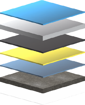
- Encapsulation / barrier
- Metal cathode (Ag, Ca/Ag) — evaporated or printed
- Electron-injection layer (PFN-Br, ZnO)
- Emissive layer (Super Yellow, F8:F8BT)
- Hole-injection layer (PEDOT:PSS)
- Transparent anode (ITO, or AgNW / PEDOT:PSS)
- Substrate (PET / PEN / glass)
Gold = slot-die coatable layers
Electrochromic devices and smart windows
(switchable glazing, adaptive displays)

- Barrier / laminate film
- ransparent electrode (ITO, AgNW, PEDOT:PSS)
- Electrolyte / ion-conducting layer (polymer gel)
- Electrochromic layer (WO₃, Nb–W oxide, electrochromic polymer)
- Transparent electrode (ITO, AgNW, PEDOT:PSS)
- Substrate (PET / glass)
Gold = slot-die coatable layers
Transparent conductive films
(ITO replacement for touch panels, heaters, electrodes))
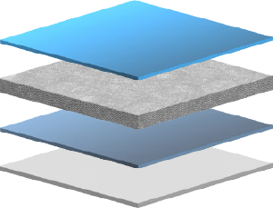
- Protective overcoat / hardcoat
- Conductive network (AgNW, PEDOT:PSS, CNT, graphene)
- Planarization / adhesion primer
- Substrate (PET / PEN / TPU)
Gold = slot-die coatable layers
Typical coating challenges
Functional layers in a printed device run from tens of nanometers to a few micrometers, and at that thickness a single defect changes how the device behaves rather than how well it performs

Ultrathin, low-defect layers
Injection and dielectric layers run below 100 nm, where a single pinhole shorts the stack or drives leakage current

Multilayer stack integrity
Each wet layer can redissolve or swell the one beneath it, mixing interfaces and dropping device performance

Air-, light- and heat-sensitive inks
Organic semiconductors and low-work-function interlayers degrade on exposure, so deposition and drying must stay enclosed and cool

Low-viscosity and particle-laden inks
Nanowire, CNT, and nanoparticle inks settle, clog, and stripe unevenly, breaking up the conductive network

Edge definition and wetting
Over-build at stripe edges interferes with lamination and device isolation, while PET, PEN, and TPU dewet without a primer

Material cost and lab-to-pilot transfer
Silver, non-fullerene, and organic semiconductor inks are expensive, and manual methods rarely transfer to wider webs without losing reproducibility
Case spotlight: slot-die coated flexible PLEDs for wearable optical sensing
Published research — Aristotle University of Thessaloniki and Organic Electronic Technologies, Greece
A research group at Aristotle University of Thessaloniki, working with the Greek organic-electronics company Organic Electronic Technologies, needed flexible polymer LEDs uniform enough to act as the light source in a wearable optical sensor. Emission color depends almost entirely on emissive-layer thickness, so the method had to hold thickness repeatably across a full web, not just a test coupon. Using a FOM roll coater, the team slot-die coated PEDOT:PSS as 13 mm stripes at 40 nm dry thickness onto a meter-long PET/ITO substrate, then coated the green emissive layer over it.
What was used
- FOM roll coater running a stripe recipe on a meter-scale flexible web
- Slot-die coated PEDOT:PSS at 40 nm dry thickness, 13 mm stripe width
- 120 µm nozzle gap, 0.045 mL/min flow, 45 °C roll, 0.5 m/min web speed
Results at a glance
- Emission color tuned to near-ideal green by coated thickness alone
- Flexible devices on a meter-scale web, comparable to rigid spin-coated references
- Finished PLEDs detected Rhodamine 6G — from coated layer to working sensor
- Builds on earlier flexible OLEDs slot-die coated on FOM equipment in ambient air
Papadopoulos et al., Nanomaterials 14(19), 1608 (2024). Open access, CC BY.

Example of flexible oledlighting panels
A solution for every stage of your research
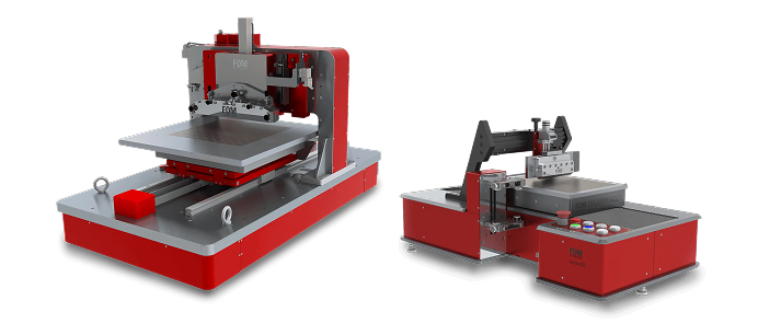
Sheet-based coating
Recipe development on small samples, with fast setup and minimal material use. Glovebox-ready for air- and moisture-sensitive materials.
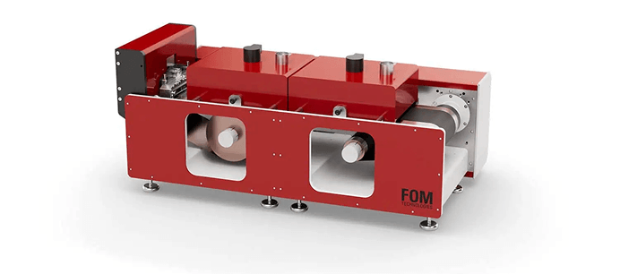
Lab-scale roll-to-roll
The bridge to continuous processing, using the same slot-die head. Longer substrates, controlled drying, and optional in-line metrology.
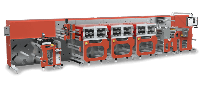
Pilot-scale roll-to-roll
Production-relevant widths and speeds, with modular options that keep your research open-ended. Build pilot data and de-risk manufacturing.

FOM’s Tensor coating software
Turns coating expertise into repeatable, scalable recipes. A clean, guided user interface takes you from setup to run with recipe-based control and storage to reuse coating protocols and test coating parameters in a structured way. The same intuitive workflow spans research tools and pilot lines, helping you scale by width and throughput without reworking your process. Advanced options—such as sequences, drying/profile management, web handling, and tension control.
Why it matters
- Save time with easy setup and reusable recipes.
- Get the same results every time with locked settings and history tracking.
- Scale with ease by using familiar software and protocols as you move from the lab to the pilot line

Expert-led training and research
FOM is staffed by scientists as well as engineers, and that team works with you directly — planning experiments, running samples, and troubleshooting the process. Whether you are new to slot-die coating or refining an established recipe, our application specialists shorten the path from a lab result to a qualified process.
- Research planning: a coating plan built around your material and constraints.
- Live training: private sessions led by a FOM scientist, online or at your site.
- Research services: we coat in the FOM laboratory and return samples with the process data.
- Book a scientist: hourly access to troubleshoot a specific issue.
- Technology demos: see a live coating run and assess it against your own materials.
Training, research services and technical resources are collected on our Science & Learning pages.
Get the application insights
Download our free application insights to see how precision coating supports solution-processed devices
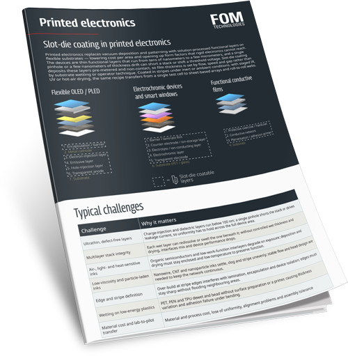
From flexible OLEDs to organic transistors, electrochromic devices, and transparent conductive films, printed electronics depends on layers thin enough that a single defect changes device behavior. This application insight sets out the four device stacks slot-die coating suits, the challenges each presents, and what it takes to carry a recipe from a test cell to a roll-to-roll web.