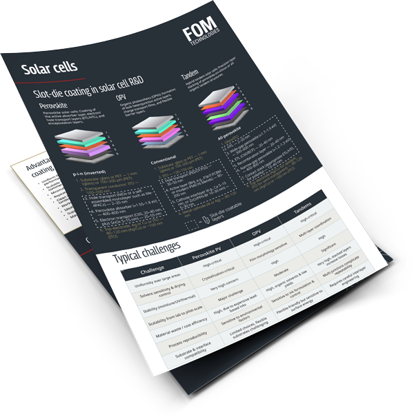
Advantages of slot-die coating in solar
Slot-die coating addresses the difficulties listed later on this page with pre-metered delivery and recipe-controlled runs, which is what makes a result on a small sample worth scaling.
Uniform films across the substrate
Unlike spin coating, slot-die deposition holds coat weight across the whole substrate, which matters more as device area grows. Fine gap control keeps films uniform on rigid glass and ITO as well as low-energy flexible polymer, across a wide viscosity range.
Controlled drying and crystallization
Programmable drying stages, including IR and hot air, allow film morphology and porosity to be tuned rather than accepted. That control is what prevents the cracking and pinhole defects common in perovskite absorber layers.
Repeatable and traceable results
Recipe-controlled parameters are logged run by run, so a successful batch can be reproduced later or in another lab without drift. The record also makes results defensible when a device goes for certification.
Low-waste, pre-metered delivery
The closed head delivers the amount of ink the target thickness requires, instead of flinging most of it off the substrate. With lead-based precursors and organic inks, that difference shows up directly in consumables spend.
Engineered clean interfaces
Precise wet gaps and optional primer layers support adhesion and well-defined interfaces between layers. In multilayer tandem cells, those interfaces set the electrical performance of the finished device.
Scale-up on the same recipe
A stable process window means a recipe developed on sheet-to-sheet can transfer to wider roll-to-roll pilot formats without being rebuilt. Width and line speed become the variables, not the chemistry.
What layers to coat with slot-die
Device architectures vary by photovoltaic technology, but slot-die coating is a core method for functional thin films that need pre-metered deposition and tight control over morphology. In the diagrams below, layers shown in gold — such as perovskite absorbers, charge transport layers (ETL/HTL), and active bulk heterojunctions — are slot-die coatable; the others are typically substrates such as glass/ITO, or top electrodes. Target thickness runs from a few nanometers to several hundred, set by ink rheology, pump speed, and drying profile.
Perovskite
Perovskite solar cells: coating of the active absorber layer, electron and hole transport layers (ETL/HTL), and encapsulation layers.

- Substrate: glass or PET — 1 mm (glass) or 100–200 µm (PET)
- Transparent conductor: ITO — 100–200 nm
- Hole transport (NiOx or a self-assembled monolayer such as Me-4PACz) — 2–20 nm
- Perovskite absorber (≈1.55–1.8 eV) — 400–800 nm
- Electron transport (C60, 20–40 nm, plus SnOx 5–15 nm) — 25–55 nm
- Top electrode: Ag, Cu, or ITO — 80–120 nm (Ag/Cu) or ~100 nm (ITO)
Gold = slot-die coatable layers
OPV
Organic photovoltaics (OPV): formation of bulk heterojunction active layers, charge transport films, and flexible barrier layers.
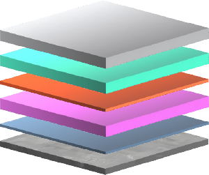
- Substrate: glass or PET — 1 mm (glass) or 100–200 µm (PET)
- ITO — 120–150 nm
- Hole transport (PEDOT:PSS) — 30–50 nm
- Active layer (BHJ, e.g. PM6:Y6 blends) — 80–200 nm
- Cathode interlayer (e.g., Ca 5–10 nm, or ZnO/PFN-Br 10–30 nm) — 5–30 nm
- Metal cathode (Al or Ag) — 80–120 nm
Gold = slot-die coatable layers
Tandem
Hybrid tandem solar cells: layer stacking for perovskite-on-silicon and all-perovskite tandem structures. In perovskite-on-silicon tandems, the same top-cell coating process (HTL, perovskite, ETL) is applied onto a pre-fabricated silicon bottom cell.
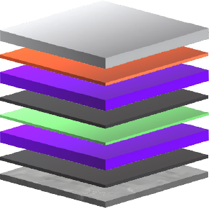
- Glass/ITO
- HTL — 2–20 nm
- Wide-gap perovskite (≈1.7–1.9 eV) — 300–600 nm
- ETL (C60/BCP) — 20–40 nm
- Recombination layer — 20–40 nm
- Narrow-gap perovskite (≈1.2–1.3 eV) — 400–800 nm
- Contact stack (ETL/HTL to suit polarity) — 10–40 nm
- Top electrode (Ag/Cu for opaque, ITO for semi-transparent) — 80–120 nm (Ag/Cu) or ~100 nm (ITO)
Gold = slot-die coatable layers
Typical coating challenges
Breakthrough efficiencies are usually demonstrated on small lab samples. Holding that performance across a larger area is where solar coating gets difficult

Uniformity over large areas
Small variations in film thickness translate directly into drops in power conversion efficiency across the device

Solvent sensitivity and drying control
Crystallization and morphology depend on the drying profile; poor control causes cracking, pinholes, and dead areas

Multilayer coordination
Tandem and multi-junction cells need interlayer engineering where each layer stays compatible with the one beneath it

Substrate and interface compatibility
Low-energy and flexible substrates resist wetting, so gap control and surface treatment decide whether a film beads or lays down

Material waste of costly inks
Spin coating discards most of what it dispenses, which is expensive with organic solvents and lead-based precursor inks

Reproducibility and scale-up
Solar films react to humidity and temperature, and a coating window that is not clearly defined introduces new defects at pilot scale
Case spotlight: QD Solar (SunDensity)
Certified record efficiency in printable solar technology using the FOM vectorSC
Canadian cleantech innovator QD Solar is developing scalable, printable photovoltaic technologies that combine high efficiency with flexible, lightweight designs. To achieve consistent, high-quality thin films and scale their research beyond the lab, they partnered with FOM Technologies.
With FOM's slot-die coating systems, QD Solar was able to iterate rapidly, test dozens of formulations, and produce large-area devices with uniform, reproducible layers while keeping material waste low. That precision and repeatability contributed directly to a certified record efficiency for their printable solar technology, a milestone for solution-processed photovoltaics.
By using FOM's tools and expertise, QD Solar is accelerating its work to bring next-generation solar technology to market.
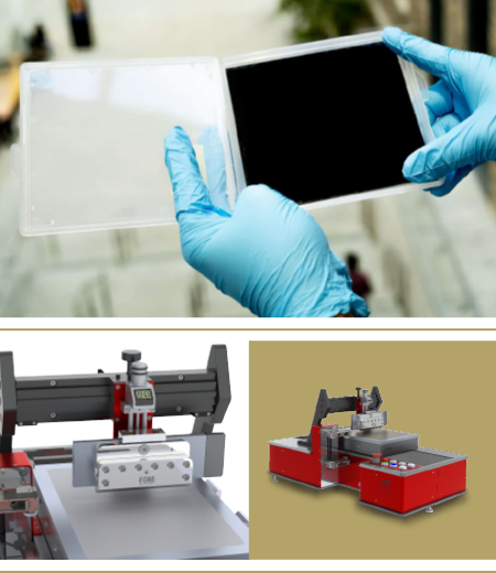
A solution for every stage of your research
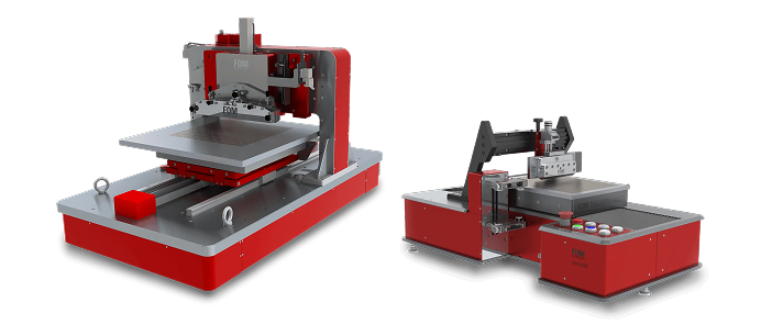
Sheet-based coating
Recipe development on small samples, with fast setup and minimal material use. Glovebox-ready for air- and moisture-sensitive materials.
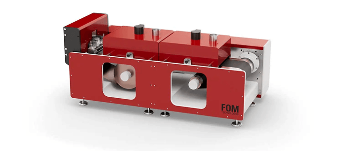
Lab-scale roll-to-roll
The bridge to continuous processing, using the same slot-die head. Longer substrates, controlled drying, and optional in-line metrology.
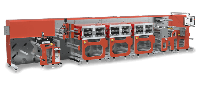
Pilot-scale roll-to-roll
Production-relevant widths and speeds, with modular options that keep your research open-ended. Build pilot data and de-risk manufacturing.

FOM’s Tensor coating software
Turns coating expertise into repeatable, scalable recipes. A clean, guided user interface takes you from setup to run with recipe-based control and storage to reuse coating protocols and test coating parameters in a structured way. The same intuitive workflow spans research tools and pilot lines, helping you scale by width and throughput without reworking your process. Advanced options—such as sequences, drying/profile management, web handling, and tension control.
Why it matters
- Save time with easy setup and reusable recipes.
- Get the same results every time with locked settings and history tracking.
- Scale with ease by using familiar software and protocols as you move from the lab to the pilot line

Expert-led training and research
FOM is staffed by scientists as well as engineers, and that team works with you directly — planning experiments, running samples, and troubleshooting the process. Whether you are new to slot-die coating or refining an established recipe, our application specialists shorten the path from a lab result to a qualified process.
- Research planning: a coating plan built around your material and constraints.
- Live training: private sessions led by a FOM scientist, online or at your site.
- Research services: we coat in the FOM laboratory and return samples with the process data.
- Book a scientist: hourly access to troubleshoot a specific issue.
- Technology demos: see a live coating run and assess it against your own materials.
Training, research services and technical resources are collected on our Science & Learning pages.
Get the application insights
Download our free application insights to see how precision coating accelerates solar breakthroughs
From perovskite to tandem and OPV, next-generation solar demands precision, scalability, and reproducibility. This application insight sets out how FOM Technologies' slot-die coating systems help researchers build high-efficiency, multilayer solar devices with less material waste, and carry a process from lab to pilot.