PEROVSKITE SOLAR CELL RESEARCH
PEROVSKITE SOLAR CELL RESEARCH
The promise of perovskite PV
Over the past decade, perovskites solar cells have attracted tremendous interest from the academic community, becoming a leading photovoltaic topic. Advances in the fundamental understanding of perovskites’ chemical and physical processes made them an attractive class of material for many researchers. In parallel, engineering developments on the architecture and fabrication of perovskite-based solar cells have resulted in an impressive growth of the cell efficiency to values over 20%. In the picture below, we show the efficiency graph from NREL for different solar technologies.

Figure 1 – Solar cell efficiency for different photovoltaic technologies over time. Perovskite cells are showing remarkable growth. (Adapted from NREL Best Research-Cell Efficiencies chart)
Across emerging PV technologies, perovskite-based cells have achieved an unprecedented rise in efficiency in a relatively short period of time. Nowadays, the efficiency is even higher than more established technologies like thin-film solar cells, including Copper Indium Gallium Selenide (CIGS), Cadmium Telluride (CdTe), and amorphous silicon (a-Si:H). In the coming years, researchers expect that the efficiency of the perovskites cells gets closer to state-of-the-art technologies like single-junction Gallium Arsenide (GaAs), paving its way to a commercially attractive technology. At the same time, these high-efficiency perovskites show promise from a manufacturing perspective, as they can be manufactured at a low cost and high speed relative to conventional PV technologies, via well-established printing and coating methods.
The importance of slot-die coating in perovskite PV
Manufacturing methods and associated production costs play an essential role when assessing any technology for industrial viability. In their final device form, perovskite solar cells can be produced in a variety of architectures, by e.g. incorporation into existent thin-film solar cells or into new architectures. However, the optimal manufacturing technique is still being determined through rigorous R&D.

Figure 2 – Typical perovskite-based solar cell structures comprising a transparent conductive oxide (TCO), an electron transport layer (ETL), perovskite layer, hole transporting layer (HTL) and a metal electrode.
Generally, the manufacturing of perovskite thin films can be achieved via vacuum or non-vacuum (i.e. solution-processing) techniques. Vacuum-based methods result in high-quality thin films, leading to the best devices performance and high manufacturing costs. On the other hand, solution-processing techniques, like spin coating or slot-die coating, tend to produce good-quality layers but with a significant advantage in terms of the low production costs and process scalability. Because spin-coating is widely available in laboratories worldwide, it has been the primary technique used to investicate solution-based deposition of these materials.
The typical deposition of the active perovskite layer occurs by either a one or two-step process. First, a precursor solution is deposited and converted to a perovskite film by applying heat in the one-step process. Alternatively, the precursor solution can be coated with a polar solvent and then quenched during the spin coating process by a non-polar solvent; this method is also known as “antisolvent”. In the two-step method, the metal halide and organic components are sequentially spin-coated on top of each other.
A significant drawback of spin coating resides in the scaling-up to larger substrates. By increasing the substrate size, it will by itself waste more considerable amounts of solutions. More than 95% of the solution is often disposed on a spin coating process, making the process not economically viable. Another important limiting factor resides in the reproducibility of the film morphology at larger scales that plays an essential role in the device’s performance and stability.

Figure 3 – a) Counted published results of different scalable deposition techniques in half-year periods since 2013. Reported PCE on aperture area below b) and above c) 1 cm2 of devices fabricated with different scalable perovskite deposition techniques plotted over time. d) Reported total power output of devices made with different scalable perovskite deposition methods plotted over time. From Bulovic, et al.
Researchers have started to recognize these limitations of spin coating-based R&D. Consequently, a rapid increase in more scalable processing technologies has taken place. In this transition, slot-die coating has proven to be a leading technology for high-quality, controllable, and scalable perovskite thin film deposition, offering excellent performance at both research and industrial scales.
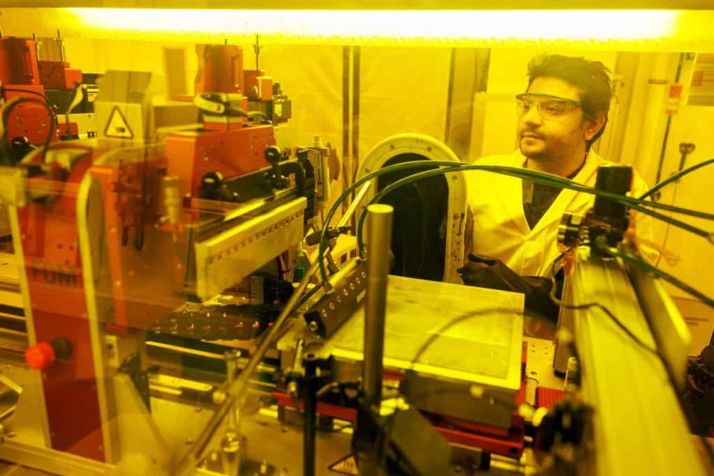
At FOM Technologies, we have been developing slot-die coaters for solution-processes perovskite research for almost a decade; providing a frontrunning solution for perovskite solar cell development via roll-to-roll and sheet-to-sheet equipment. It is our mission to offer an unmatched combination of precision, control, and scale in the high-quality thin-film coating to enhance the impact of research in this field and accelerate this technology towards commercialization. The FOM vectorSC and alphaSC sheet-based benchtop slot-die coaters are our most popular products for perovskite PV development, owing to their ability to coat on both rigid (e.g. silicon wafers or glass encapsulation) and flexible (e.g. PET foil) substrates, as well as N2 knife add-on accessory for controllable gas quenching of the perovskite layer.

Figure 4 – FOM alphaSC used for perovskite solar cells development. Options like air knife technology are available.
What is next for perovskites?
The development of perovskite solar cells has been remarkable over the last decade. This development will likely accelerate in the coming years due to extensive funding available to combat climate change, where solar energy plays an important role. Research activities are likely to focus on reducing the layer’s defects, identifying new, more environmentally friendly materials, and improving long-term device durability. At FOM, we will continue to support our academic customers in advancing their R&D needs and keeping our corporate customers to pave the way to large-scale production
Read more on the topic
Download the FOM Technologies Product brochure
Fill in your information and click download to access the pdf.


