THE ROLE OF SLOT-DIE COATING IN THE FUTURE OF PHOTOVOLTAICS
SLOT-DIE COATING IN THE FUTURE OF PHOTOVOLTAICS

Download: Bridging the Gap: Scalable Research in Photovoltaics from Lab to Industry
Access Dr. César Omar Ramírez Quiroz’s presentation slides by filling in your information and clicking download.
Short abstract to the topic
Solar cells, crucial for reducing global CO2 emissions, must reach a capacity of 70 TW by 2050 for a swift transition to renewables. Silicon technologies dominate, boasting well-established supply chains, processes, and markets. However, enhancing power conversion efficiency (PCE) while maintaining cost-effectiveness remains challenging.
Tandem solar cells, combining two cells to capture different parts of the sunlight spectrum, offer promise. Silicon-perovskite tandems, particularly, show potential for efficiency gains. Perovskite-based materials could disrupt efficiency while aligning with current manufacturing methods, offering a rapid solution to climate change.
This review examines fabrication routes for perovskite-based photovoltaics’ industrial integration, focusing on non-concentrated tandem designs. Challenges include processing decisions, but slot-die coating emerges as a scalable and efficient solution. Its potential for rapid processing on non-flat substrates makes it strategic for advancing the field.
Current scenario for solar energy
Since the invention of the steam engine marked the onset of the industrial revolution, humans have emitted a cumulative amount of no less than 1.5 X 10¹² tons of CO2. In recent years the annual additions are around 36 X 109 tons of CO2, with expectations of increasing every year as demographics and industrialization grow globally. As different scientific reports predict, a failure to dramatically cut emissions to zero will bring catastrophic effects on the atmosphere with an increment in temperature of up to 4 °C by the end of the century. To this end, a rapid transition to a 100% renewable energy economy is the best strategy for accomplishing the targets set by the Paris agreement [1–3].
Solar cells or photovoltaics are at the center of the main strategies for reducing global CO2 emissions. The estimated needed global PV generating capacity should be about 70 TW by 2050 to significantly impact a quick transition to renewables within an acceptable timeframe. 70 TW by 2050 corresponds to 6-10 kW of photovoltaics per capita and an annual production of PV systems of 3-4 TW. Currently dominating the market, Silicon technologies are critical for achieving this goal. While supply chain, well-established standard processes, products, Levelized cost of electricity (LCOE), bankability, and markets [1–3] are in the best shape and up to the challenge, one of the most important questions remains unanswered – how to integrate further improvements in power conversion efficiency (PCE) without disrupting cost-effectiveness.
Different mainstream and emerging technologies are already reaching expected practical power conversion efficiency values. For example, the highest recorded efficiency of a functional single-junction silicon solar cell is 26.7% (180 cm2, designated area), obtained under an interdigitated back contact (IBC) silicon heterojunction (HJ) configuration. The cell was developed by Kaneka in Japan, employing high-quality thin-film HJ passivation technology and low-resistance electrodes [4]. Similar technology driven by the same laboratories yielded a record 24.4% in a larger area (13,177 cm2, module designated area). However, despite constant improvements, silicon-based PV efficiencies remain lower than the theoretical efficiency limit of a single-junction silicon solar cell (32.33% [5] or 29.43% when accounting for other realistic theoretical considerations [6]).
High power conversion efficiency has never been as crucial as it is today, not only for accomplishing the global environmental targets but also for the survival itself of the PV industry. The survival of the PV industry is a concept not visible at first glance, but it becomes more evident when accounting for the service life of the already installed solar cells. In this way, PV production does not only have to grow to satisfy the global environmental targets but also to renew existing installations reaching their end of life and in need of decommissioning and replacement.
Concepts such as multijunction and tandem solar cells have been part of the PV technology roadmap for a long time. Tandem solar cells consist of two solar cells stacked on top of each other, where the two cells efficiently collect complementary sections of the sunlight spectrum. Tandem photovoltaic modules with silicon bottom cells offer a promising route to exceed the single-junction photovoltaic efficiency limit. Amongst all the tandem partner technologies for silicon, perovskites-based materials have the potential to deliver a technological disruption in efficiency while maintaining compatibility with current manufacturing protocols. Hence, making silicon-perovskites the fastest route to enhance the silicon market and rapidly address climate change [7]. In addition, perovskites have the potential of vastly reducing the cost of raw materials and manufacturing, likely introducing a window of opportunity for disrupting existing solar supply chains. Being the fastest growing technology in photovoltaics, it has reached efficiencies of up to 25.7% since its first report in 2009 [8]. One of the challenges facing this development is manufacturing strategies to fabricate add-on perovskite technologies where scalability, cycle-time, and stability will be of decisive importance for large-scale deployment and market entry.
Perovskite-based tandems; Setting the stage
To summarize the previous section, solar energy is one of the more abundant, reliable, and attractive power generation sources at our disposal. Solar is at the center of the few options for addressing climate change, but it faces critical challenges. Worldwide solar production capacity would have to grow by 30-fold to keep the PV industry from collapsing while meeting the milestones required by the Paris agreement. For this reason, increments in power conversion efficiency have never been as critical as they are today. The realization and deployment at a large scale of tandem architectures could be the answer. Perovskite solar cells can be a vital driver for electricity cost reduction through improvements in the Levelized cost of electricity (LCOE).
The record efficiency for multi-junction solar cells, at a laboratory scale, is 39.2% under one-sun illumination and 47.1% under concentrated illumination (143 suns) [9], [10]. This cell comprises six junctions fabricated on a monolithic stack and electrically connected, forming a parallel circuit. The researchers at the National Renewable Laboratories in the USA (NREL), behind these efforts, relied on III-V materials (so-called because of their position on the periodic table) for constructing such devices. Each of the six junctions (the photoactive layers) is specially designed to capture light from a specific part of the solar spectrum.
To address which technology is best suited as a top-cell for silicon-based tandems, Zhengshan (Jason) Yu et al. analyzed the spectral response of different candidates [11]. This study reveals that the higher efficiencies can render GaAs the best top cell. Therefore, III-V silicon tandem-cell partners would seem a natural guide in developing efficient silicon-based tandems. However, III-V cells rely on epitaxial growth for bandgap design. Epitaxial crystal growth is an approach not easily transferable to silicon because of its unique constant crystal lattice. Albeit the continuous effort to reduce the cost of manufacturing these solar cells, the overall cost is still several orders of magnitude above where they need to be for terrestrial applications. Hence, III-V solar cells are primarily employed in high-end applications like powering satellites. Despite their economic feasibility, these concepts elucidate a clear picture of what is possible. On that account, perovskites are the best top-cell material in terms of cost-performance.
A summary of different perovskite-based tandem technologies is displayed in Figure 1 (left-hand side). For example, Helmholtz Zentrum Berlin (HZB) recently reported a record efficiency of 29.8% Silicon-perovskite tandem solar cell at a lab-scale [12]. As a different approach, Nanjing University, in collaboration with the University of Toronto, has reported an all-perovskite tandem device with a certified record efficiency of 26.4%, also at a lab-scale size typically smaller than 1 cm2 [13]. The advent of perovskite-based photovoltaic is also reflected in highly regarded industry reports such as the International Roadmap for Photovoltaic (ITRPV). The ITRPV highlights development trends, and it is considered a guide for the entire crystalline silicon-based photovoltaic supply chain [14]. A summary roadmap for the expected efficiency of different perovskite-based tandem technologies is depicted in Figure 1 (right-hand side panel). The ITRPV 2020 [15] report shows a high trust in perovskites. The values published by this report are average stabilized efficiency accounting for mass production. Alongside the ITRPV perovskite-technology roadmap, we added the most relevant scientific advancements academia has offered since their discovery.

Figure 1 – Left-hand side; perovskite-based tandem solar cells efficiency time evolution. Right-hand side; cumulative efficiency trend for perovskite-based photovoltaics on different classifications. E.g., semitransparent (ST) perovskite solar cells (PSC), lab-scale (an active area smaller than 10 cm2), or large scale (an active area greater than 10 cm2). Additionally, triangles summarize the expectation of mass production efficiencies for different tandem cell concepts [15] — figure design modified from reference [16] with information partly extracted from the latest edition of the International Roadmap for Photovoltaics (IRTPV) [15].
The PCE time evolution depicted on the right-hand-side panel of Figure 1. Show perovskite technologies can comfortably deliver the efficiency levels predicted by the IRTPV in tiny samples or lab scale. Therefore, while the topic of size and scale is a conversation that will follow, we will regard it as a large scale to anything larger than 10 cm2. When considering more realistic measures, the whole picture changes, revealing an earlier question on integrating one of the fastest developed technologies in history into current mass production protocols. A more detailed time evolution of what we call large-scale perovskite solar cell devices is illustrated in Figure 2 (left-hand-side panel).
Slot-die coating, perovskites, and the topic of scale
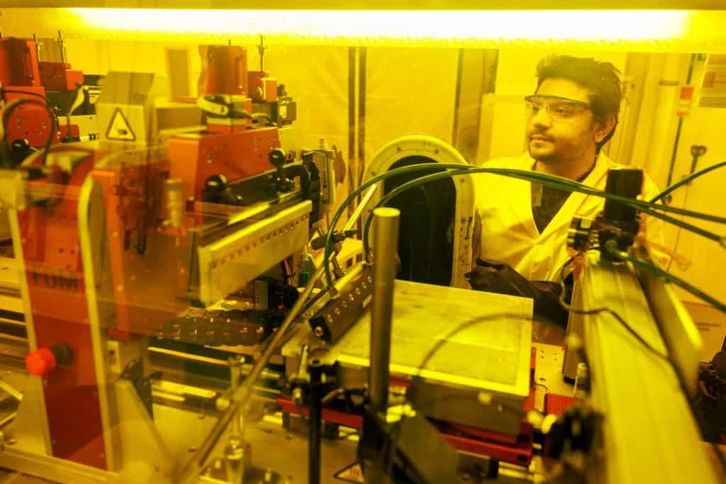
To begin understanding the topic of scalability, we must start by looking back on the last 12 years of research. Figure 2 (right-hand-side panel) shows a breakdown of PCE time evolution divided by the deposition technique used to coat the perovskite layer. Up to the current efficiency record, it is no secret that we scientists like spin-coating. Spin-coating is a coating method that relies on a centrifugal force for depositing uniform thin films on flat surfaces. Typical speeds for perovskite deposition protocols range in the thousands of revolutions per minute (rpm) for the ideal conditions to favor layer quality. Notably, the substrate size is the more critical limitation of relying on centrifugal forces to generate the necessary liquid-vapor interface for film deposition. In other words, spin-coating is intrinsically unscalable, on the relevant sizes at least (more on that later). The second-best strategy for perovskite deposition is slot-die coating. Slot-die coating is the scalable deposition method holding the highest efficiency record in tiny sizes (lab scales) and has the highest efficiency record in 10 cm2 or larger (see Figure 2).
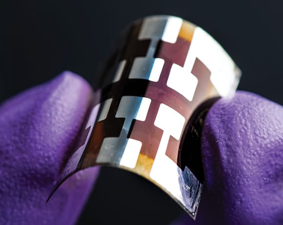
Slot-die coating is a deposition technique for fabricating homogeneous wet films from a dissolved material into a wide variety of substrates, rigid or flexible. Firstly, a pumping element drives the solution into the slot-die head component. Next, the solution gets distributed through an ink manifold and later guided along the slot-head length and into a meniscus guide and a shim mask. Finally, the formation of a meniscus bridges the downstream solution flow with a moving substrate generating a continuous wet film. As the width of the slot-die head defines the width of the printing area, and a combination of the flow rate and the substrate speed determines the thickness, the target film specifications can be pre-metered. Therefore, the coating size in slot-die is intrinsically unlimited, where lengths of 2 meters are commonly spotted in industrial sites.
Co-evaporation is in second place amongst the scalable perovskite deposition techniques. Co-evaporation can too be extrapolated and envisioned as deployed at GW scale PV factories. However, critical hindrances might arise from energy consumption, CAPEX expenditures, and manufacturing cycle time. To elucidate on the last two, we need to consider the necessary time to deposit a perovskite thin-film (around 500 nanometers thick) ranging from 100 minutes (latest record efficiency 20.6% [17]) to almost 8 hours (to our knowledge, one of the most extended cycle times reported to date[18]). The longer the cycle time, the larger the capacity of the production line would have to be to match the current machine tooling for silicon fabs. A higher CAPEX is just a linear consequence.

Figure 2 – Left-hand side; single-junction perovskite solar cells- efficiency evolution on a large scale (with an active area greater than 10 cm2) – An FOM AlphaSC is used to fabricate the latest record [19]. Right-hand side; single-junction perovskite solar cells- efficiency evolution (all sizes) by deposition method used for the perovskite absorber – As notable exceptions, we included slot-die coating efforts with the utilization of FOM tools, see references [19] and [20] (red, white-filled squares). — figure design modified from reference [16].
To address the topic of scale, it is necessary to discuss further the current mainstream technologies. A broad spectrum of silicon solar cell manufacturing technologies drives the photovoltaic industry. However, a few trends are anticipated toward fewer processing steps. Currently, the transition from p-type to n-type Silicon wafers is underway. By the end of 2020, p-type wafers still dominated the market. The latter is mainly due to their reliability and ease to manufacture. But this is outweighed by other advantages of n-type wafers. N-type wafers will obtain lower light-induced degradation and significantly higher efficiencies, which is a most relevant advantage. According to the IRTPV 2020 report, the market share of n-type wafers will increase successively, dominating in less than ten years [15].
The situation with cell formats is somewhat diverse. The production facilities for wafers, cells and modules are partly fixed to specific geometries so that there are mutual persistence effects. Today, the most commonly used cells have the format 166 x 166 mm2 (M6). They will, step by step, be replaced by 210 x 210 mm2 (M12). In today’s transition phase, several intermediate formats play significant roles, some of which differ by only a few millimeters. The PERC technology (passivated emitter and rear cell) has dominated for a few years now. It is assumed that this will remain the case for the next ten years. Significant changes are not seen. Bifacial modules are a relatively new trend with a market share of about 25%. In the case of typical utility-scale systems, higher electricity yields can be achieved if the light is scattered onto the back (or albedo) of the modules. Whether the additional costs for the modules and the system mounting are worth it is still under discussion. However, their market share is expected to increase [21]. The standard silicon photovoltaic cell is a PERC cell made of Czochralski mono-crystalline n-type silicon with at least 166 x 166 mm2 (M6) format. The modules may have the bifacial feature or maybe monofacial as well—both result in modules and photovoltaic systems with optimum Levelized cost of energy (LCOE).
This author elaborated a graphical summary depicted in Figure 3. A simple correlation of size vs. power conversion efficiency illustrates the distance between the state-of-the-art and the suitable size for silicon-wafer-based PV, that is, from M0 to M12 wafer sizes. The most straightforward multi-junction configuration that provides efficiency gains without adding high cost to the balance of systems is a non-concentrated tandem design. Two sub-cells of inexpensive solar absorbers with different bandgaps are combined. Several challenges are evident in accomplishing this, and strategic decisions regarding processing seem unclear. However, the performance-size evolution shows the multiple advantages of using slot-die coating. A clear path for scalability, potential short cycle times, and easy processing on non-flat substrates make slot-die coating a strategic choice for moving the field forward.

Figure 3 – Outstanding efficiency-scale research efforts across different scalable deposition methods. Spin-coating, a non-scalable technique, is included as a benchmark. Additionally, the typical wafer size for silicon solar cell manufacturing and the ITRPV-2021 [15] predicted module sizes for residential and power plants as reference. — figure design modified from reference [16].
Your Title Goes Here
References and author
Author: César Omar Ramírez Quiroz
- Hemetsberger, W., Schmela, M. & Chianetta, G. Gobal Market Outlook for Solar Power, 2020-2024. (2020) doi:10.4018/978-1-7998-4607-9.ch006.
- Hans-O. Pörtner (Germany), Debra C. Roberts (South Africa), Helen Adams (United Kingdom), Carolina Adler (Switzerland/Chile/Australia), Paulina Aldunce (Chile), Elham Ali (Egypt), Rawshan Ara Begum (Malaysia/Australia/Bangladesh), Richard Betts (United Ki, Z. Z. I. (Malaysia). Climate Change 2022 – Impacts, Adaptation and Vulnerability – Summary for Policymakers. Ipcc (2022).
- Verlinden, P. J. Future challenges for photovoltaic manufacturing at the terawatt level. J. Renew. Sustain. Energy 12, (2020).
- Yoshikawa, K. et al. Silicon heterojunction solar cell with interdigitated back contacts for a photoconversion efficiency over 26%. Nat. Energy 2, 17032 (2017).
- Shockley, W. & Queisser, H. J. Detailed balance limit of efficiency of p-n junction solar cells. J. Appl. Phys. 32, 510–519 (1961).
- Richter, A., Hermle, M. & Glunz, S. . Crystalline Silicon Solar Cells Reassessment of the Limiting Efficiency for Crystalline Silicon Solar Cells. IEEE J. Photovoltaics 3, 1184–1191 (2013).
- M. Schmela, B. Clark, H. Máté, C. Lits, and R. R. Global Market Outlook for Solar Power 2021-2025. (2021).
- Kojima, A., Teshima, K., Shirai, Y. & Miyasaka, T. Organometal halide perovskites as visible-light sensitizers for photovoltaic cells. J. Am. Chem. Soc. 131, 6050–1 (2009).
- Geisz, J. F. et al. Building a Six-Junction Inverted Metamorphic Concentrator Solar Cell. IEEE J. Photovoltaics 8, 626–632 (2018).
- Geisz, J. F. et al. Six-junction III–V solar cells with 47.1% conversion efficiency under 143 Suns concentration. Nat. Energy 5, 326–335 (2020).
- Yu, Z., Leilaeioun, M. & Holman, Z. Selecting tandem partners for silicon solar cells. Nat. Energy 1, (2016).
- Tockhorn, P. et al. Nano-optical designs enhance monolithic perovskite / silicon tandem solar cells toward 29.8% efficiency. Res. Sq. (2022).
- Xiao, K. et al. All-perovskite tandem solar cells with 24.2% certified efficiency and area over 1 cm2 using surface-anchoring zwitterionic antioxidant. Nat. Energy 5, 870–880 (2020).
- International Technology Roadmap for Photovoltaic (ITRPV) – vdma.org – VDMA. https://www.vdma.org/international-technology-roadmap-photovoltaic.
- International Technology Roadmap for Photovoltaic (ITRPV) 2020 Results. VDMA Photovolt. Equip. 12, 1–83 (2021).
- Ramírez Quiroz, C. O. Full thin-film tandems solar cells – Industry perspective. in Outcome of PERCISTANDs first scientific workshop (2021).
- Roß, M. et al. Co-Evaporated p-i-n Perovskite Solar Cells beyond 20% Efficiency: Impact of Substrate Temperature and Hole-Transport Layer. ACS Appl. Mater. Interfaces 12, 39261–39272 (2020).
- Qiu, L. et al. Hybrid chemical vapor deposition enables scalable and stable Cs-FA mixed cation perovskite solar modules with a designated area of 91.8 cm2 approaching 10% efficiency. J. Mater. Chem. A 7, 6920–6929 (2019).
- Li, J. et al. Anti-Ribbing: Ink Optimization Enables Certified Slot-Die Coated Perovskite Solar Cells with > 22% Certified Power Conversion Efficiency and a Full Year Outdoor Stability. SSRN Electron. J. (2021) doi:10.2139/ssrn.3971152.
- Li, J. et al. 20.8% Slot-Die Coated MAPbI3 Perovskite Solar Cells by Optimal DMSO-Content and Age of 2-ME Based Precursor Inks. Adv. Energy Mater. 11, (2021).
- IRENA. Future of solar photovoltaic: Deployment, investment, technology, grid integration and socio-economic aspects (A Global Energy Transformation: paper). International Renewable Energy Agency vol. November (2019).
Read more on the topic
Pioneering solar research using FOM coaters
Discover how Dr. Janardan Dagar became the a Staff Scientist at HZB, where they have many FOM slot-die coaters in use for solar cell research.

FOM Talks: QD Solar Inc.
We met up with QD Solar Inc. to talk about their latest record-breaking result, their use of FOM equipment, and the potential of slot-die coating in cutting-edge green technology in general.
Slot-die coating in perovskites solar cells research
Perovskites solar cells are a hot topic in photovoltaics. In this post, we discuss how slot die coating plays a vital role....